GROUP
Energy Saving Device Development Group
Advancing research and development of
diamond semiconductor
- Group Leader
- Professor Norio Tokuda
- Fields of Specialty
- condensed matter physics, electrical and electronic engineering, inorganic materials chemistry, energy-related chemistry
- Keywords
- Next generation semiconductor, quantum device, diamond, crystal growth, plasma
The two pillars which are key to realizing the IEA’s 450 Scenario are energy conservation and renewable energy. Our group is engaged in the development of diamond semiconductor, a key technology for energy conservation.
Mainstream silicon semiconductors are approaching their performance limit. The development of new materials is advancing: among them, diamond has the highest breakdown field, carrier mobility and thermal conductivity, making it the ultimate semiconductor material.
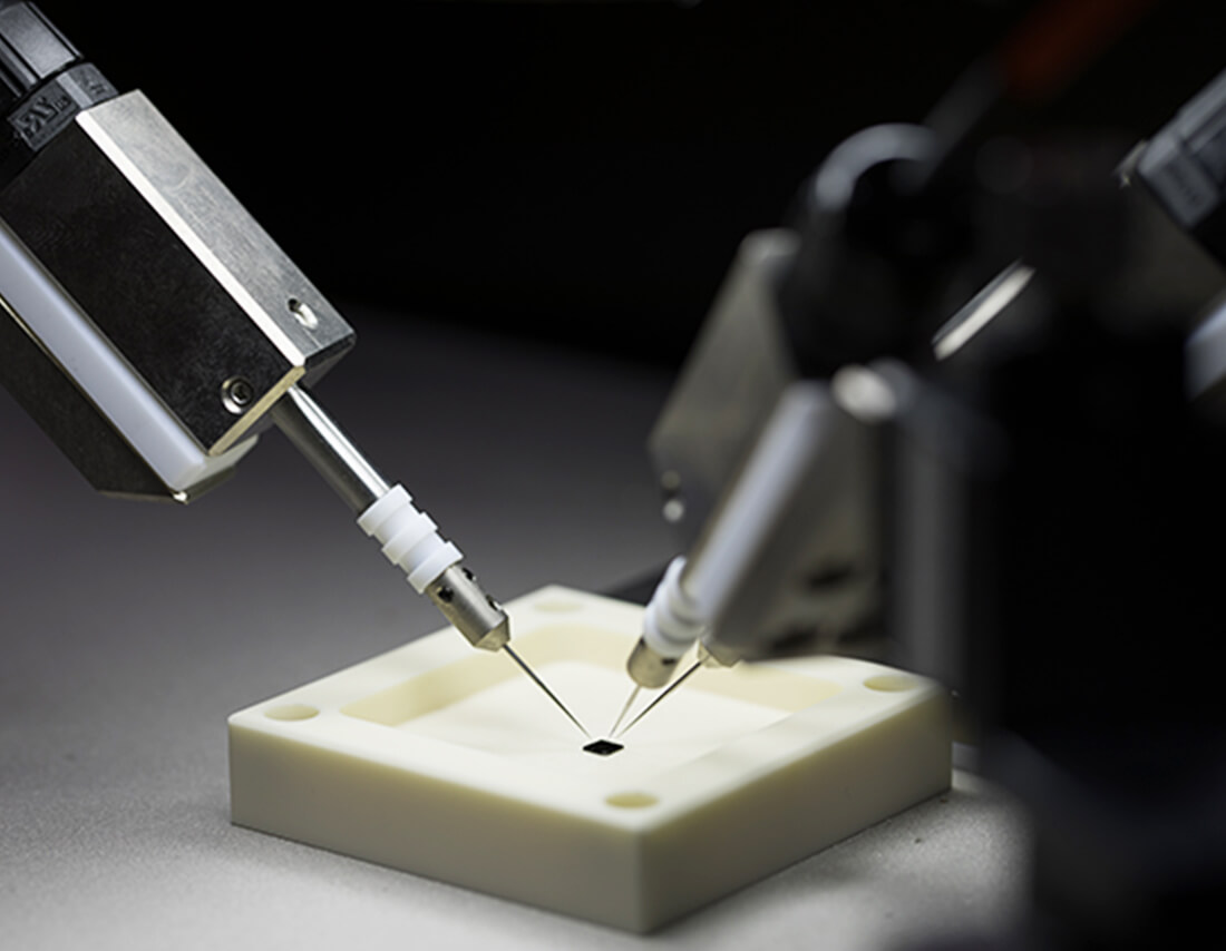
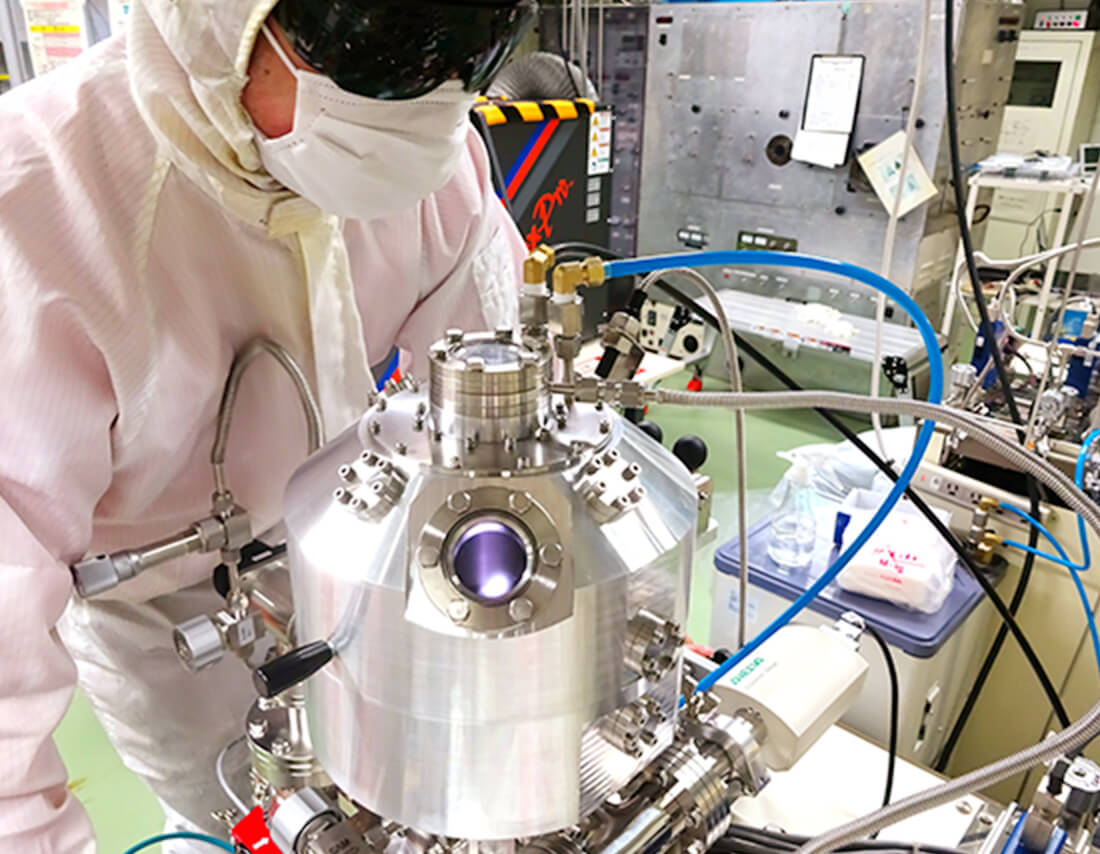
Our group’s strength is surface and interface structure control technology, which realizes the lateral growth of flat diamond membranes at the atomic level. We are engaged in the research and development of all technological elements for the sequence processing of preparing diamond ingots and processing them into wafers. Our achievements to date include the development of the world’s fastest diamond growth technology, the creation of the world’s first inversion layer diamond (MOSFET), and the successful demonstration of its operation. We have also developed a high speed etching technique using a carbon solid-solution reaction of nickel, and are opening the way for device processes. We are proud of our world-leading research standard, as a hub for diamond semiconductor research.
From now, we plan to establish a technique and framework for realizing half-inch monocrystal wafers combined with minimal fab, in order to achieve early stage social implementation of power devices.